Not known Details About Fast CCD - Advanced Photon Source

 Catalytic Combustion Detector (CCD)
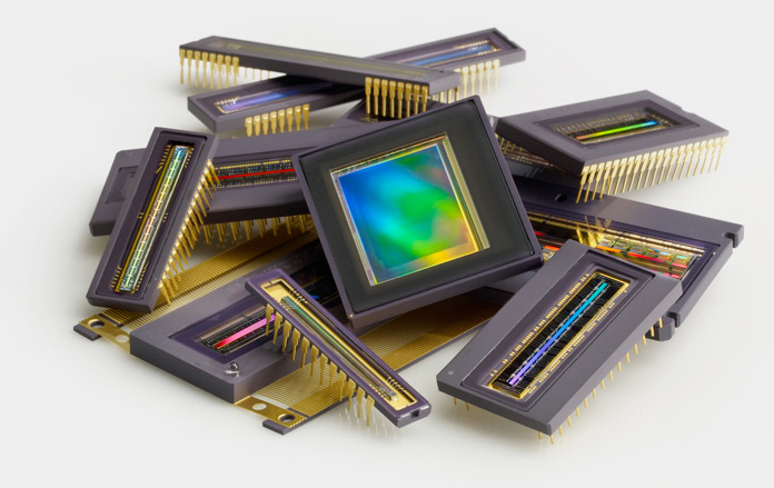 Ocean Optics Spectrometer Linear CCD Sensor Toshiba TCD1304DG TCD1304Ap Detector - eBay
Examine This Report about Understanding Binning in High Energy CCD Detectors - Andor
A one-dimensional variety, utilized in line-scan cameras, records a single piece of the image, whereas a two-dimensional selection, utilized in video and still cams, catches a two-dimensional picture representing the scene forecasted onto the focal plane of the sensor. When the array has actually been exposed to the image, a control circuit triggers each capacitor to transfer its contents to its next-door neighbor (operating as a shift register).
By duplicating this process, the controlling circuit transforms the entire contents of the array in the semiconductor to a series of voltages. In a digital gadget, these voltages are then sampled, digitized, and usually saved in memory; in an analog device (such as an analog video cam), they are processed into a constant analog signal (e.
by feeding the output of the charge amplifier into a low-pass filter), which is then processed and fed out to other circuits for transmission, recording, or other processing. Detailed physics of operation [edit] Charge generation [modify] Prior to the MOS capacitors are exposed to light, they are prejudiced into the depletion region; in n-channel CCDs, the silicon under the predisposition gate is a little p-doped or intrinsic.
Nevertheless, it takes time to reach this thermal stability: as much as hours in high-end scientific cameras cooled at low temperature level. At first after biasing, the holes are pushed far into the substrate, and no mobile electrons are at or near the surface area; the CCD thus operates in a non-equilibrium state called deep depletion.
Product note: Renishaw RenCam CCD detector (pdf) - Truths
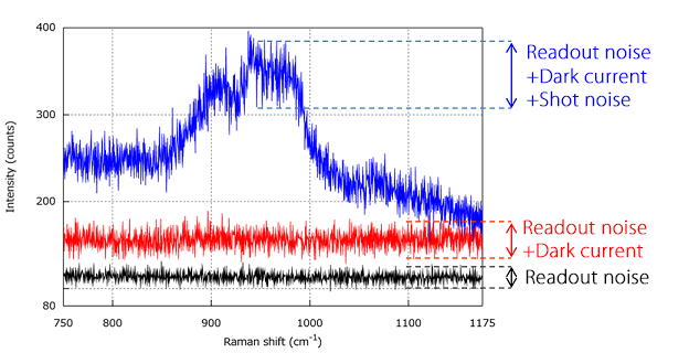
4 pair-generation processes can be identified: photo-generation (up to 95% of quantum effectiveness), generation in the exhaustion area, generation at the surface area, and generation in the neutral bulk. The last 3 processes are referred to as dark-current generation, and add noise to the image; they can restrict the total usable integration time.
In this case, the well is said to be full. Need More Info? of each well is referred to as the well depth, usually about 105 electrons per pixel. Style and production [modify] The photoactive region of a CCD is, normally, an epitaxial layer of silicon. It is lightly p doped (normally with boron) and is grown upon a substrate product, frequently p++.